
In semiconductor manufacturing, every scrapped wafer wastes electricity, water, and chemicals. Siemens’ Brian Taylor states that sustainability “is not a separate track” from yield and throughput. The most efficient fab is, by this measure, the most sustainable one: fewer defects mean less energy burned and less waste produced.
As Brian Taylor of Siemens put it, sustainability “is not a separate track.” It’s embedded in every conversation about yield, throughput, and cost. In a business where every wafer demands enormous energy, water, and chemical input, sustainability is now a function of how efficiently a fab converts resources into finished products.
What Does a Scrapped Wafer Actually Cost?
A scrapped wafer is both a production failure and a sustainability failure. Every defective wafer represents wasted electricity, water, and chemicals consumed during fabrication. By treating yield loss as an environmental metric, fabs can quantify sustainability in operational terms: a one-percent yield improvement in a high-volume fab translates directly into measurable reductions in carbon footprint and resource use.
Every scrapped wafer represents wasted electricity, water, and materials — and in modern fabs, those costs are staggering. What was once dismissed as yield loss now doubles as a sustainability failure.
By reframing yield as part of environmental performance, fabs can quantify sustainability in operational terms: fewer defects mean less energy burned, fewer chemicals consumed, and less waste produced. The equation is simple — the more efficient the process, the greener the operation.
This perspective shifts sustainability from compliance to competitiveness. A one-percent yield improvement in a high-volume fab doesn’t just lift profit margins — it translates directly into measurable reductions in carbon footprint and resource use.
How Do Digital Tools Track Fab Sustainability?
Simulation and analytics tools now allow semiconductor fabs to model energy flows, process efficiency, and waste streams in real time. These tools run millions of digital scenarios to test process improvements. As Brian Taylor of Siemens explains, sustainability data and production data live on the same platform: “It’s not a different tool, it’s a different representation of how we serve that information to the user.”
The complexity of semiconductor production once made sustainability nearly impossible to track in real time. Water recycling, energy consumption, and chemical recovery — all were monitored in isolation, if at all.
That’s changing through digitalization. Today’s fabs are increasingly using simulation and analytics tools to model energy flows, process efficiency, and waste streams. These tools run millions of digital “what-if” scenarios to test improvements — optimizing how energy and resources are consumed at every step.
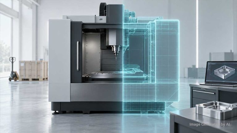
A key advantage of this approach is that sustainability data no longer lives in a separate system. It becomes part of the same digital twin or data platform used for operations. Plant managers can toggle between a production view and a sustainability view without switching tools — one lens showing yield and uptime, the other showing water, energy, and emissions impact.
As Brian Taylor explains, “It’s not a different tool — it’s a different representation of how we serve that information to the user.”
Why Do Fab Teams Still Work in Silos?
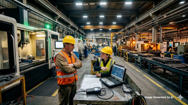
In many semiconductor fabs, the sustainability lead and the plant manager still operate separately. Engineers focus on process uptime and yield; sustainability managers focus on corporate carbon goals and compliance. Digital transformation changes this: when both teams access the same data covering energy use, yield rates, and tool efficiency, they discover shared metrics and common goals that improve both operations and environmental performance.
In many fabs, the sustainability lead and the plant manager still operate in parallel worlds. The engineer focuses on process uptime and yield, while the sustainability manager looks at corporate carbon goals and compliance.
Digital transformation is collapsing that divide. When both teams access the same data — energy use, yield rates, tool efficiency — they discover shared metrics and common goals.
As these departments connect, the insights multiply: sustainability teams learn how process efficiency affects carbon outcomes, while engineers gain visibility into how their production choices shape environmental performance. The result is not just better reporting, but smarter operations across the board.
How Do Fabs Scale Sustainability Globally?
Scaling sustainability across sites and countries requires unified dashboards that compare water reuse rates, emissions, and equipment efficiency across regions. Siemens and its partners support fabs using these global platforms, allowing corporate sustainability teams to scorecard multiple facilities, identify best practices, and meet growing demands from customers and regulators for transparency into how components are manufactured.
The next step is scaling sustainability across sites and countries. Siemens and its partners are already supporting fabs that use unified dashboards to compare performance across regions — tracking water reuse rates, emissions, and equipment efficiency globally.
This shift allows corporate sustainability teams to scorecard multiple facilities against each other, identifying best practices and bottlenecks. It also reinforces trust and traceability — a growing demand from both customers and regulators who want transparency into how components are made.
Is Efficiency the Same as Sustainability in Fabs?
Sustainability in semiconductor manufacturing is not about using less in absolute terms. It is about producing more within the same resource envelope. Fabs that treat energy, water, and yield as interconnected performance levers, rather than separate metrics, are finding that operational efficiency and environmental goals reinforce each other directly.
Sustainability in semiconductors is no longer about using less — it’s about producing more with the same resource envelope. The fabs that succeed will be those that understand that energy, water, and yield are not separate metrics but interconnected levers of performance.
The fabs that treat sustainability as an operational discipline — not a PR metric — are discovering something profound: when efficiency and environmental goals align, both profit and purpose accelerate.
The most sustainable fab, it turns out, is simply the most efficient one.
About the author
 This article was written based on insights shared by Brian Taylor, Head of Electronics & Semiconductor US at Siemens, during a CXO Series interview. Sponsored by Siemens.
FAQ
1. What is the connection between yield and sustainability in semiconductor manufacturing?
In semiconductor manufacturing, yield and sustainability are directly linked. Every scrapped wafer wastes the electricity, water, and chemicals consumed during its fabrication. A one-percent yield improvement in a high-volume fab translates into measurable reductions in carbon footprint and resource consumption. Siemens’ Brian Taylor describes sustainability as “not a separate track” from yield and throughput.
2. How do simulation and analytics tools help fabs track sustainability?
Simulation and analytics tools allow fabs to model energy flows, process efficiency, and waste streams in a single platform. Rather than monitoring water recycling, energy consumption, and chemical recovery in isolation, plant managers can toggle between a production view and a sustainability view within the same system. Siemens supports this approach so operational and environmental data share one data platform.
3. Sustainability reporting vs. sustainability operations: what is the difference in semiconductor fabs?
Sustainability reporting tracks compliance metrics after the fact; sustainability operations embeds environmental performance into daily production decisions. In fabs using shared data platforms, engineers and sustainability managers access the same yield, energy, and tool-efficiency data. This integration means process choices are evaluated for their environmental impact in real time, not only in quarterly compliance reports.
4. How can semiconductor fabs compare sustainability performance across multiple global sites?
Fabs can use unified dashboards to track water reuse rates, emissions, and equipment efficiency across multiple regions simultaneously. Siemens and its partners support global platforms that allow corporate sustainability teams to scorecard facilities against each other, identify best practices, and surface bottlenecks. This approach also provides the traceability that customers and regulators increasingly require from semiconductor supply chains.
Related Reading
How to Scale AI in Manufacturing
Feedstocks, Funding, and the Future: What’s Holding Back Industrial Decarbonization
Why Every Semiconductor Fab Needs a Digital Twin Strategy , Not Just Digital Tools