In semiconductor fabs, progress has long been measured in nanometers. But the next great leap isn’t happening on the wafer — it’s happening in how factories see, think, and respond. Artificial intelligence is quietly reshaping inspection, maintenance, and operational decision-making, marking a shift from human reaction to digital foresight.
From Human Vision to Machine Intelligence
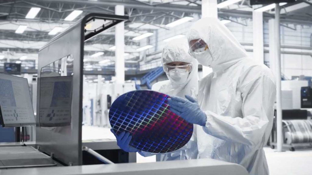
For decades, visual inspection in fabs relied on the human eye or so-called pixel counters — systems that did little more than flag anomalies by comparing brightness and color patterns. These approaches often slowed production with false positives, forcing expensive manual rechecks.
The cost wasn’t just time: every unnecessary pause disrupted the delicate cadence of high-volume fabrication. The human eye, no matter how experienced, fills in missing visual data — introducing errors that can ripple through an entire production run.
AI vision systems are ending that era. They can now learn in minutes what once took months, training on as few as five images to distinguish between acceptable variations and genuine defects. Subtle lighting changes or minor shading no longer trigger costly false alarms. The result: faster throughput, fewer reworks, and higher yield.
Inspection That Learns — and Keeps Learning
The breakthrough isn’t just accuracy — it’s adaptability. These new AI-driven systems continue learning as they operate, turning every wafer, every camera feed, into a data source that sharpens performance.
For an industry where margins and tolerances are microscopic, that continuous learning creates resilience. When lighting shifts, product mixes change, or environmental factors fluctuate, the system recalibrates instantly. The fab no longer needs to stop to adjust; the system adjusts itself.
Predictive Maintenance Enters the Chat
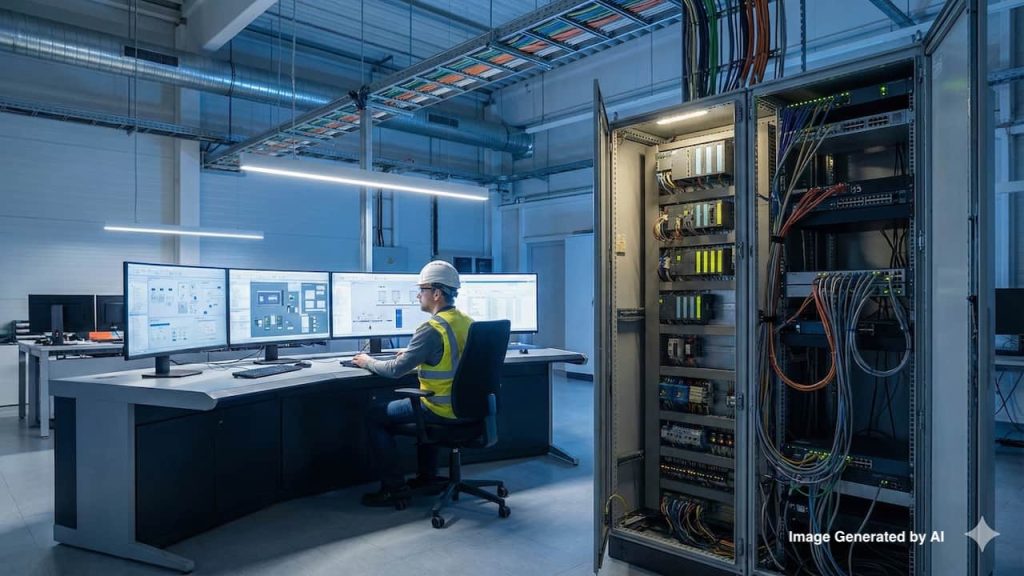
A similar transformation is unfolding in fab maintenance. Predictive AI now monitors thousands of process variables — pressure, vibration, flow, temperature — to identify deviations long before equipment fails.
But what truly changes the game is the way engineers interact with these systems. Instead of sorting through dashboards or raw logs, they can type or say: “Why is the etching chamber temperature rising?” or “Show maintenance trends for Tool 27.”
The AI responds with contextual insights, often accompanied by graphs or step-by-step diagnostics. It’s intuitive, multilingual, and practical — a Copilot-like experience that simplifies decision-making for operators who may not be data scientists.
This conversational interface bridges the gap between advanced analytics and the real-world demands of fab operations. It makes predictive maintenance not just powerful, but usable.
From Reaction to Foresight
In a semiconductor fab, every minute of downtime carries a heavy cost. When predictive maintenance systems shorten troubleshooting cycles or prevent unplanned shutdowns, the return is immediate and measurable.
AI is also building a new form of capital — operational intelligence. Every inspection image, sensor reading, and maintenance log feeds into a growing data ecosystem that continuously improves the system’s accuracy and reliability.
This creates a feedback loop that gets smarter over time, enabling fabs to move from reactive firefighting to proactive optimization.
A Glimpse Into the Next Phase
The integration of AI inspection and predictive maintenance with digital twins is already on the horizon. Entire production lines will soon be simulated virtually, stress-tested digitally, and optimized continuously.
When that happens, the physical and digital fabs will operate as one — predicting, simulating, and self-correcting in real time.
For now, though, the shift already underway is profound. The move from manual inspection and reactive repair to AI-driven vision and predictive foresight marks a fundamental redefinition of how fabs operate.
The New Competitive Edge
AI in the semiconductor industry is a new operational discipline. Fabs adopting these systems are already reporting sharper visibility, fewer false alarms, and higher uptime.
Those still relying on legacy inspection methods risk falling behind, not just in productivity but in insight. In an industry that can no longer afford to be reactive, the fabs that “see” through AI are setting a new standard — one where intelligence, not intuition, drives precision.
About the author
 Brian Taylor is a seasoned leader in the semiconductor industry, serving as Head of Semiconductor Sales / Head of Electronics & Semiconductor US at Siemens. With more than 20 years at Siemens, his expertise spans advanced manufacturing, automation architecture, and digitalization—focused on helping customers in the high-cost, high-complexity semiconductor ecosystem accelerate productivity and yield.
Sponsored by Siemens